Engineering the Digital Heart of Excellence.
Our in-house SMT facility represents the pinnacle of electronics manufacturing. We don't just assemble products; we manufacture the proprietary logic that ensures professional-grade stability for every unit.
Explore SMT Precision
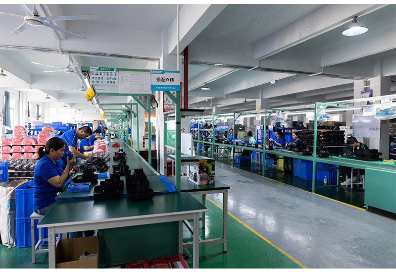
Standardized SMT Workflow
Solder Paste Printing
Using ultra-fine stencils to apply precise solder paste volumes for flawless conductivity.
3D SPI Inspection
Solder Paste Inspection (SPI) checks height and volume in 3D to prevent 90% of potential defects.
High-Speed Mounting
Yamaha/Juki pick-and-place machines ensure micron-level component alignment at 100,000+ CPH.
Reflow Soldering
Controlled 10-zone heat profiles create robust, oxidation-free solder joints for long-term stability.
Automated AOI
Post-reflow Automated Optical Inspection (AOI) catches the smallest anomalies before final assembly.
Environmental Integrity for Peak Reliability.
A single speck of dust can compromise a circuit. That’s why our SMT workshop operates under a strict Class 10,000 cleanroom protocol, where temperature, humidity, and static electricity are monitored 24/7 to ensure flawless solder joint integrity.
The Limits of Precision
Handling ultra-miniature passive components with high-speed accuracy.
Micron-level repeatability for complex BGA and QFN packaging.
Supporting high-density multi-layer PCBA designs for smart controls.
100% compliant with global environmental and food-safety standards.
Advanced Production Environment & Machinery.
High-Speed Mounting
Utilizing Yamaha/Juki high-precision mounters to achieve micron-level accuracy at high-volume speeds for zero-defect placement.
3D AI Inspection
Real-time automated optical inspection (AOI) driven by AI algorithms to catch bridges, polarity, and soldering defects instantly.
Thermal Precision
10-Zone Nitrogen Reflow technology provides stable heat profiles, ensuring unbreakable and oxidation-free solder joints.
Full-Line Automation
Integrated automated loading and unloading systems minimize human interference for a continuous, error-free production flow.
Inside our Precision Manufacturing Floor.
Partner with Our SMT Experts.
Need a customized PCBA solution for your next kitchen appliance project? Whether it's a proprietary control logic or a smart sensor integration, our in-house SMT facility provides the speed, precision, and IP protection you require.
We help transform your electronic sketches into professional, market-ready PCBA layouts.
Accelerate your R&D with fast-turnaround board assembly for prototype verification.
Every custom board undergoes full Automated Optical Inspection to ensure zero field failures.
Strict NDA protocols ensure your proprietary code and circuit designs remain exclusively yours.
SMT & PCBA Expertise FAQ.
Our advanced Yamaha/Juki lines are capable of handling PCB sizes up to 510mm x 460mm. For specialized oversized boards, we can provide custom carrier solutions to maintain micron-level placement precision.
Absolutely. 100% of our production lines are configured for lead-free processes. We use high-grade SAC305 solder paste and nitrogen-purged reflow ovens to meet the strictest global environmental and food-safety standards.
Every board passes through our AI-driven 3D AOI (Automated Optical Inspection) and SPI (Solder Paste Inspection). For hidden joints like BGA, we utilize X-Ray inspection to ensure zero-voiding and perfect structural integrity.
For standard prototyping with all components in stock, our fast-track service can deliver PCBA samples within 3-5 working days. Mass production lead times typically range from 2-4 weeks depending on component complexity and volume.
